Design & specifications#
If you want to know how BeagleV-Fire board is designed and what are it’s high-level specifications then this chapter is for you. We are going to discuss each hardware design element in detail and provide high-level device specifications in a short and crisp form as well.
Tip
For hardware design files and schematic diagram you can checkout BeagleV-Fire GitLab repository: https://git.beagleboard.org/beaglev-fire/beaglev-fire
Block diagram#
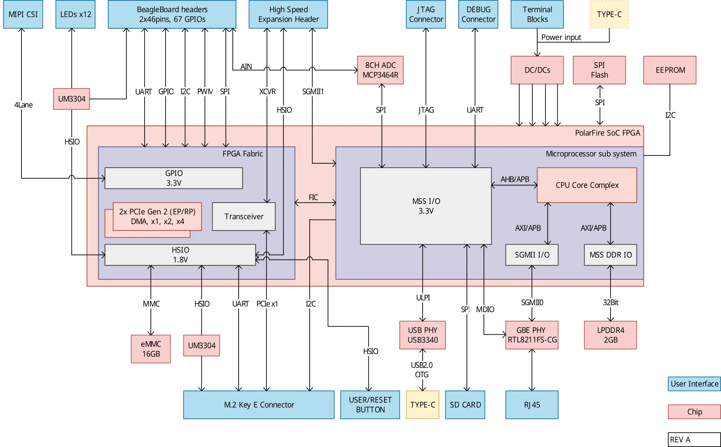
Fig. 302 System block diagram#
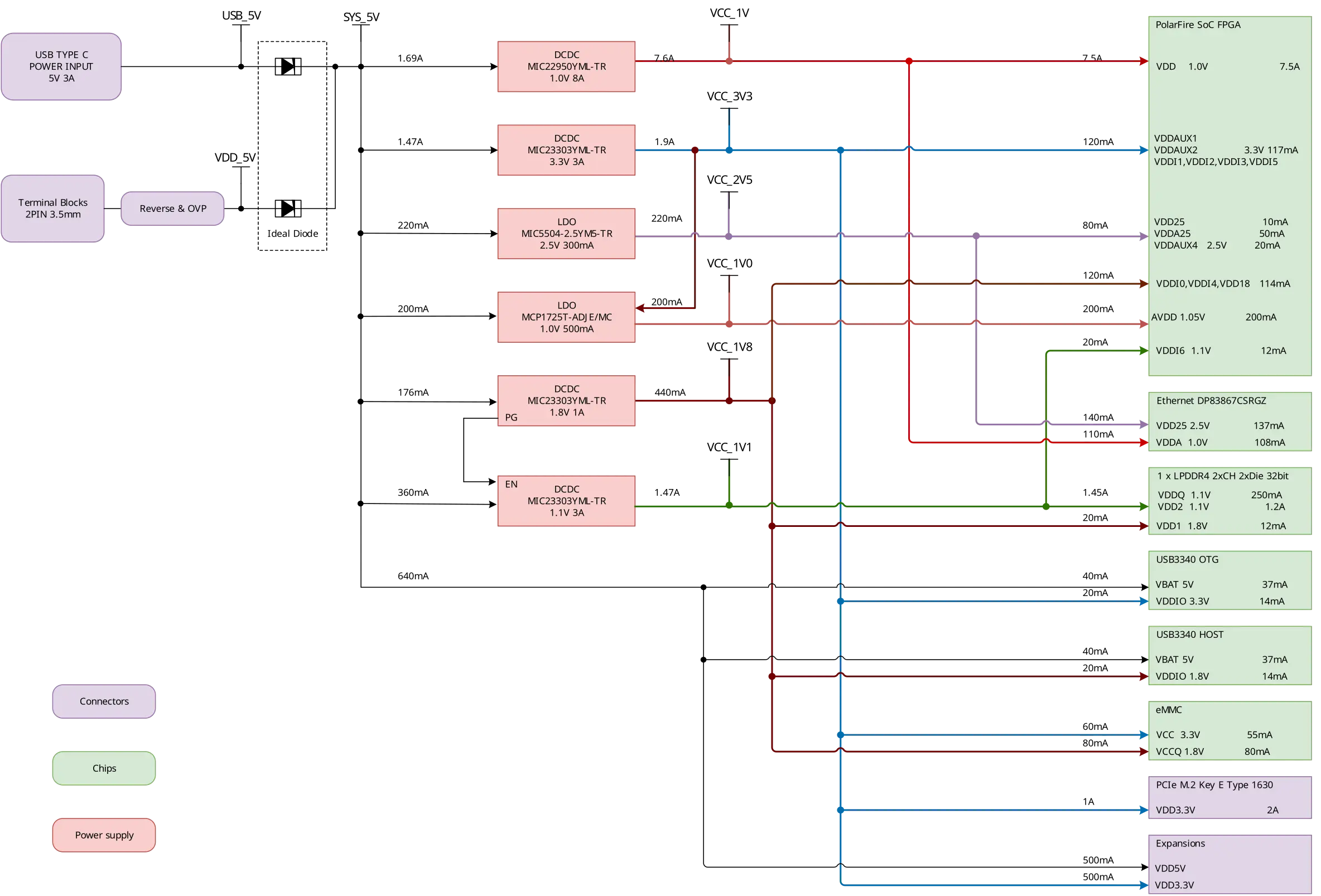
Fig. 303 Power tree diagram#
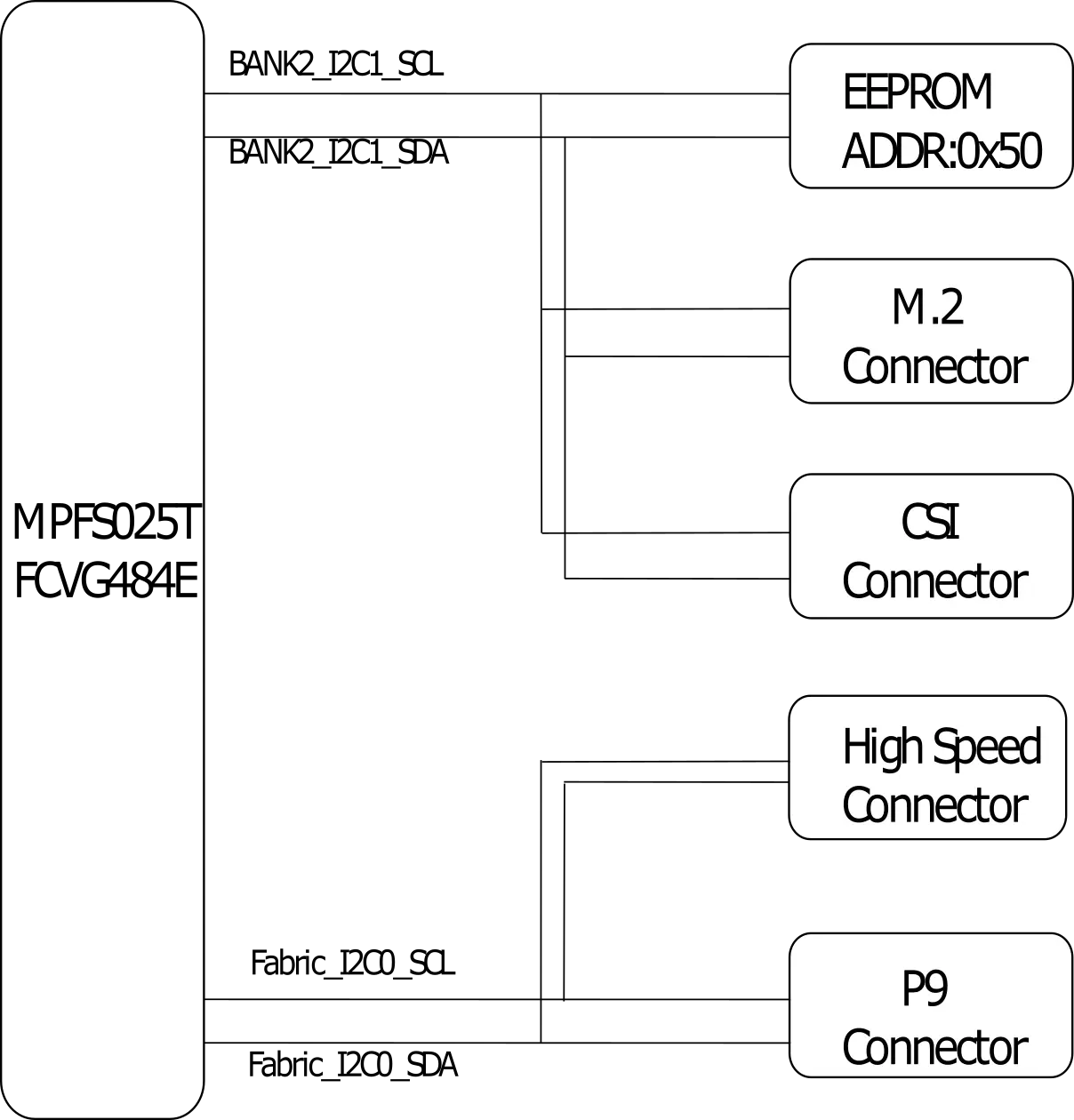
Fig. 304 I2C tree diagram#
System on Chip (SoC)#
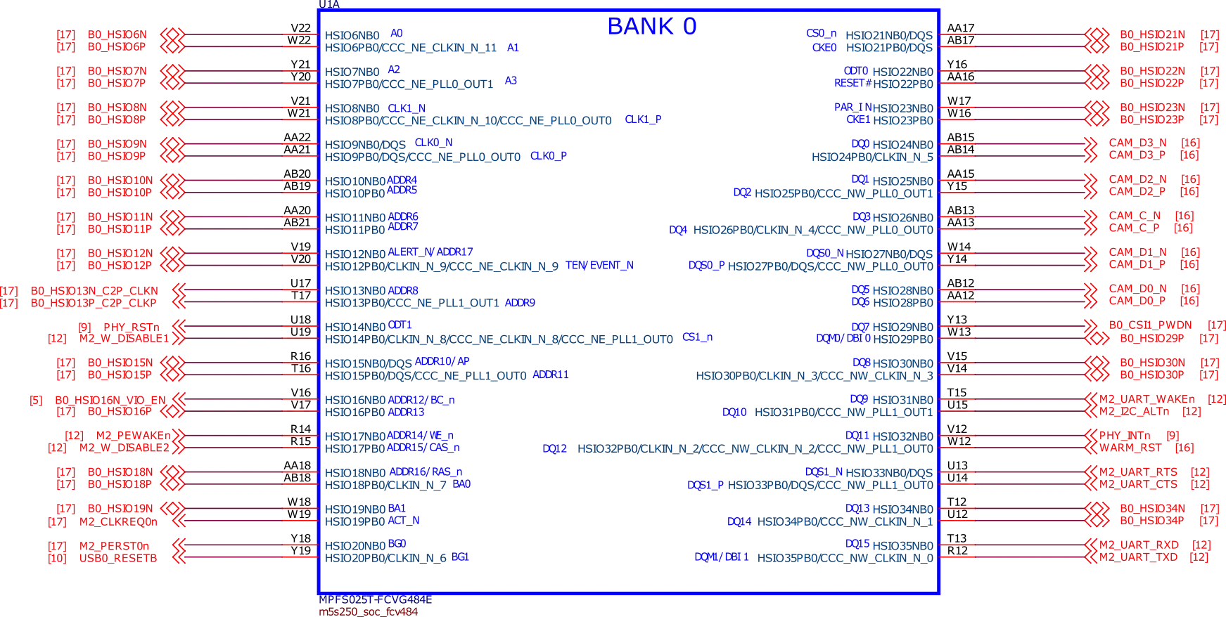
Fig. 305 SoC bank0#
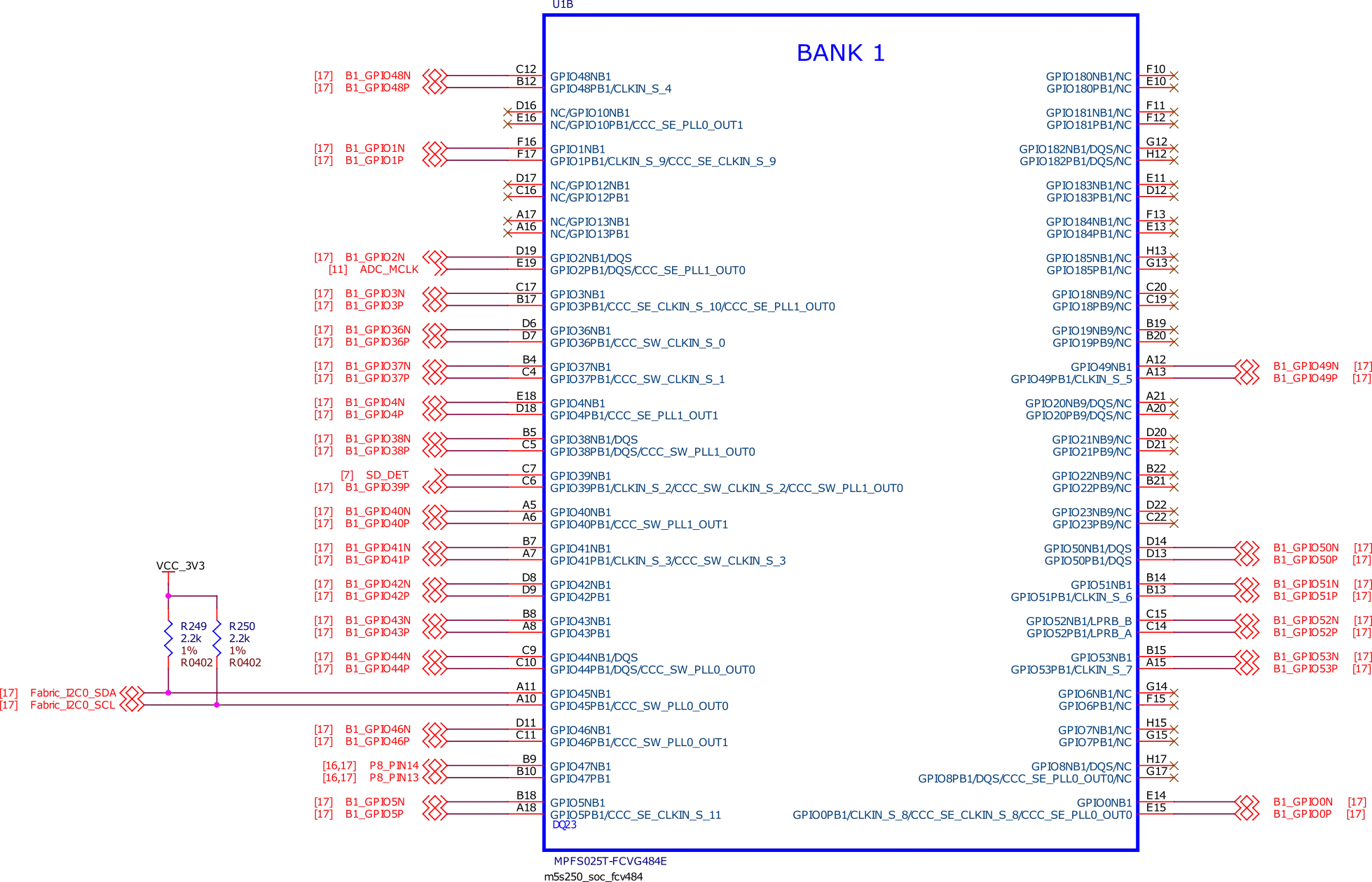
Fig. 306 SoC bank1#
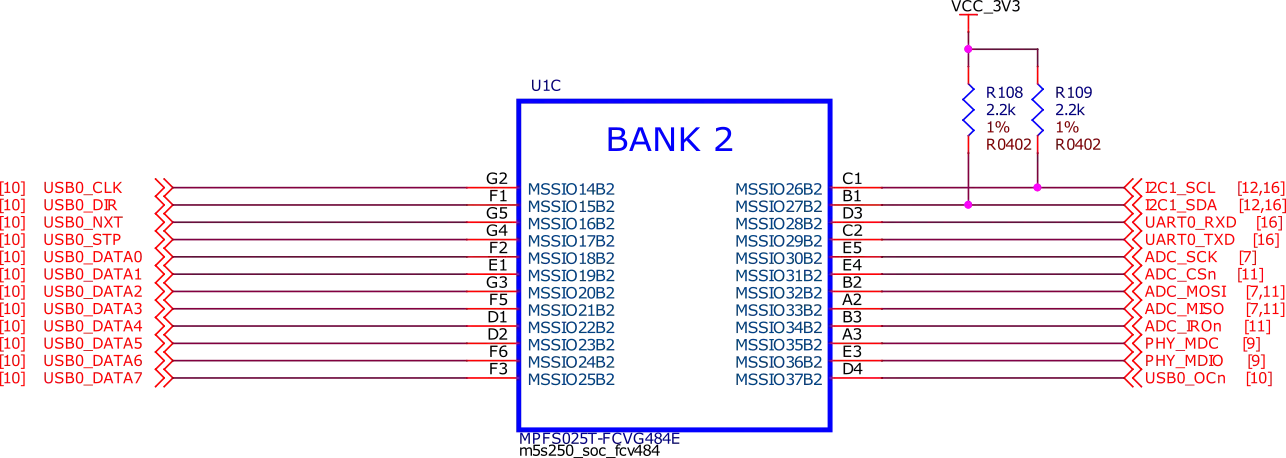
Fig. 307 SoC bank2#
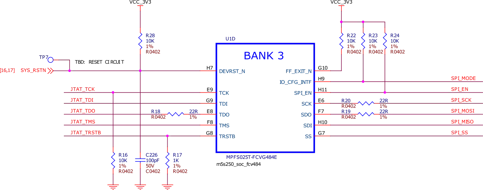
Fig. 308 SoC bank3#
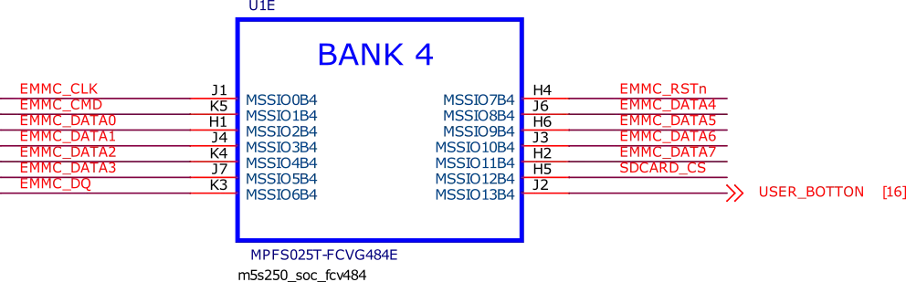
Fig. 309 SoC bank4#
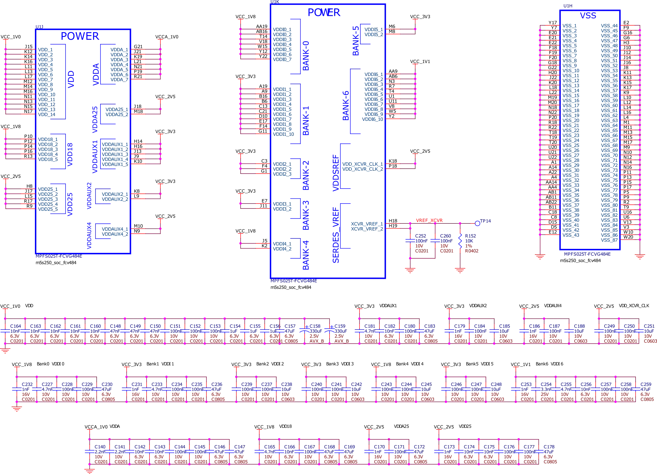
Fig. 310 SoC power#
Power management#
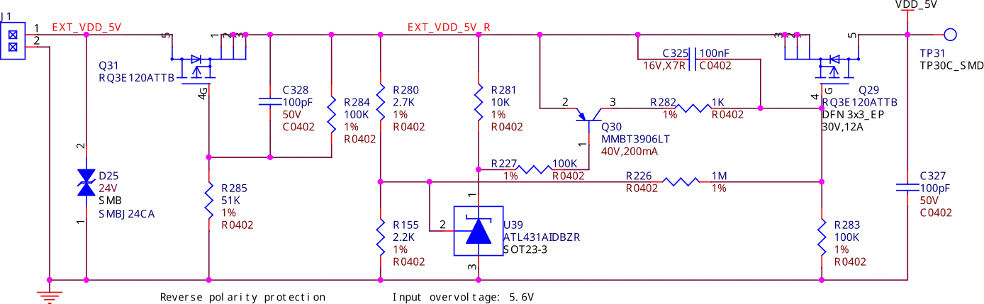
Fig. 311 DC 5V input#
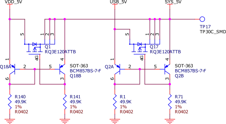
Fig. 312 Ideal diode#
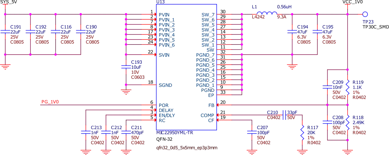
Fig. 313 VCC 1V0#
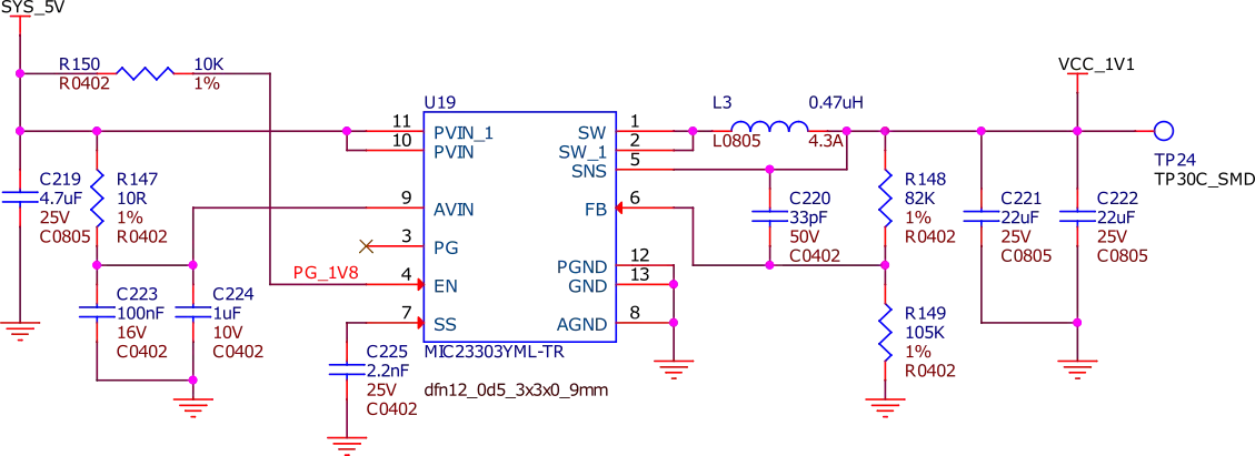
Fig. 314 VCC 1V1#
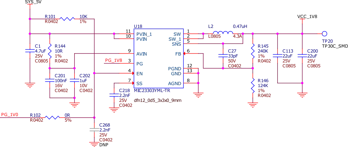
Fig. 315 VCC 1V8#
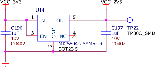
Fig. 316 VCC 2V5#
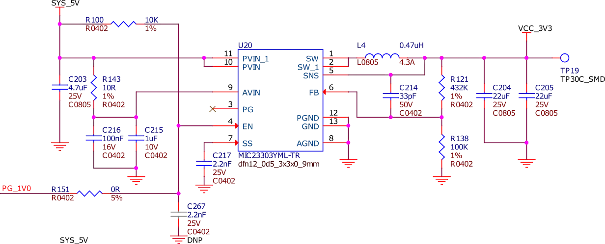
Fig. 317 VCC 3V3#
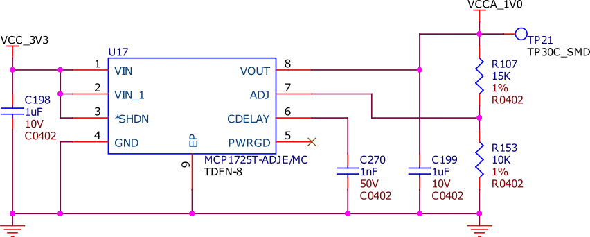
Fig. 318 VCCA 1V0#
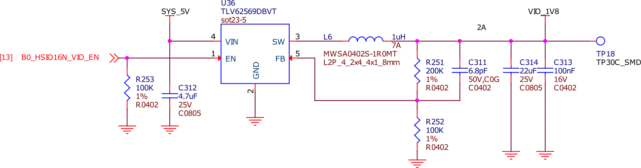
Fig. 319 VIO enable#
General Connectivity and Expansion#
USB-C port#
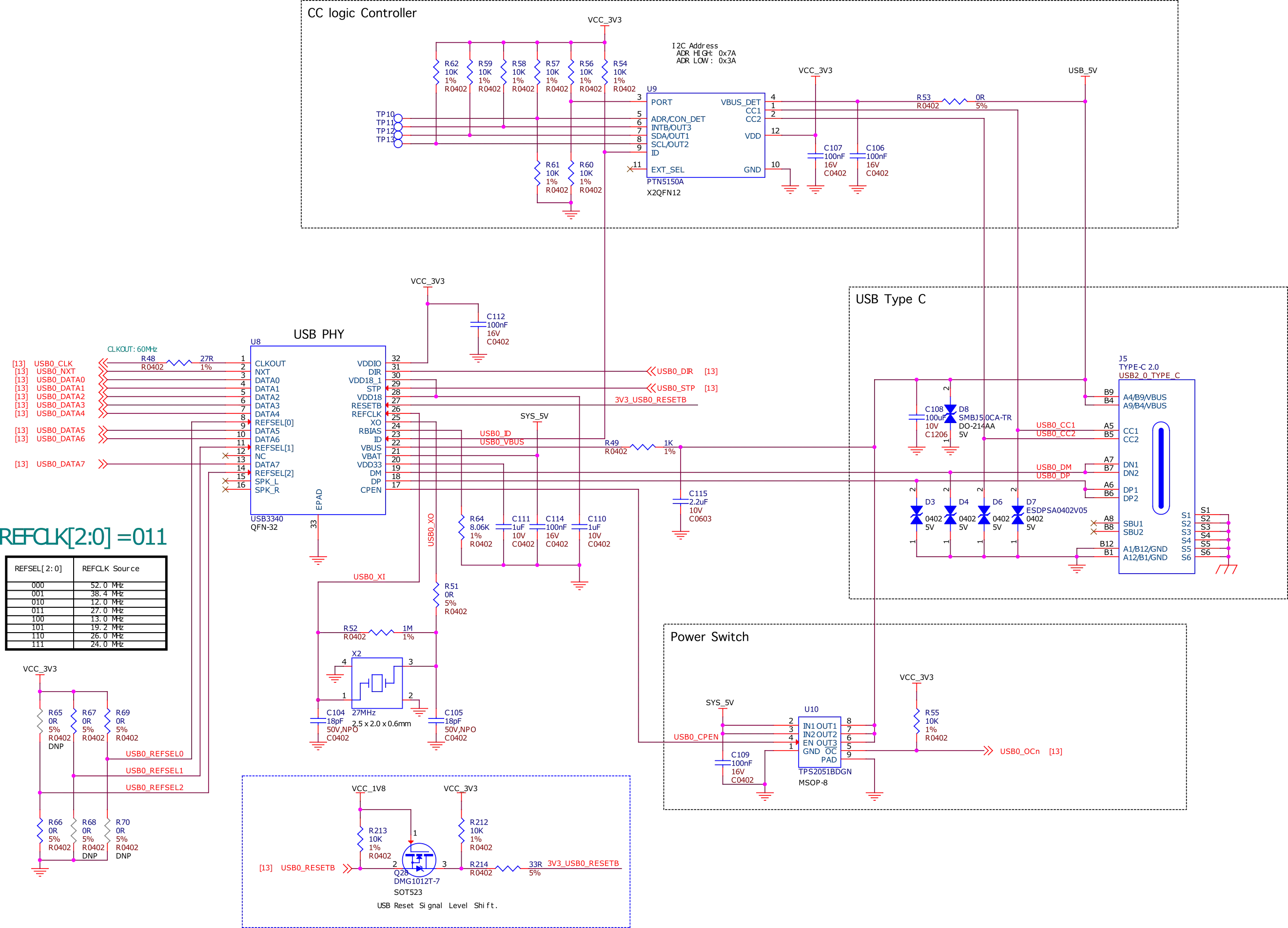
Fig. 320 USB C#
P8 & P9 cape header pins#
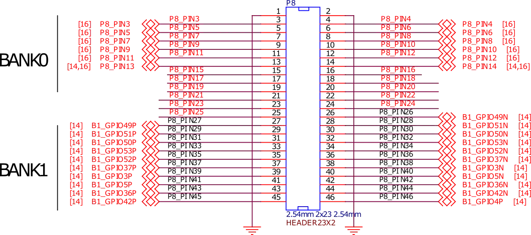
Fig. 321 P8 cape header#
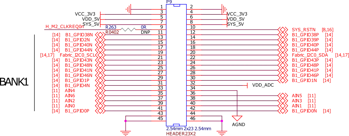
Fig. 322 P9 cape header#
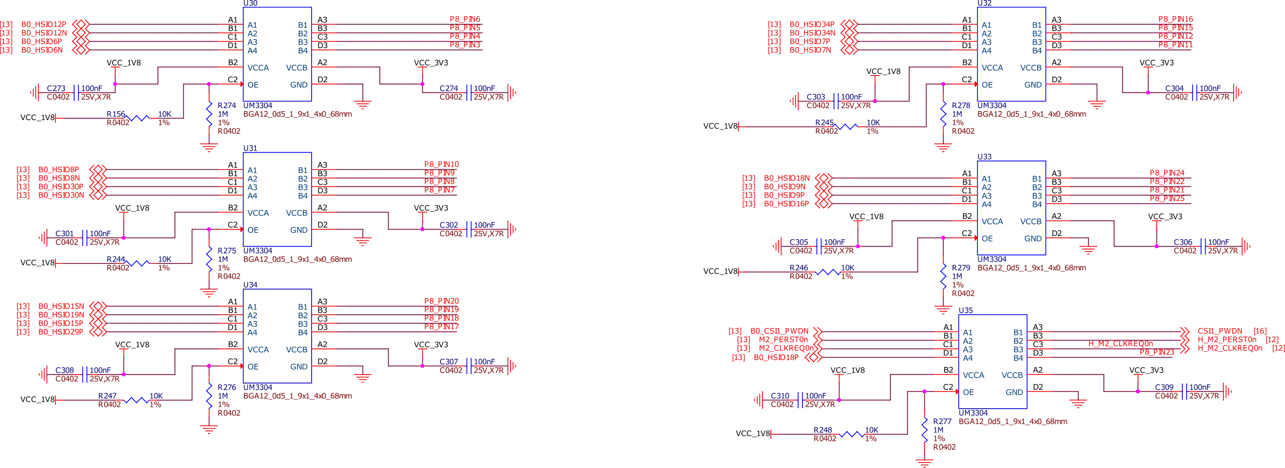
Fig. 323 Cape header voltage level translator#
ADC#
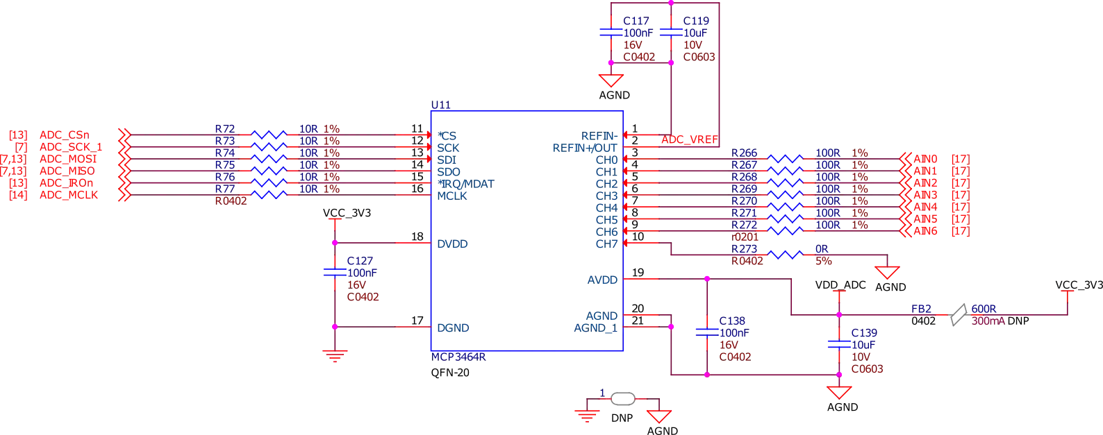
Fig. 324 16bit Delta-Sigma ADC#
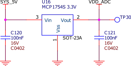
Fig. 325 ADC LDO power supply#
Buttons and LEDs#
User LEDs and Power LED#
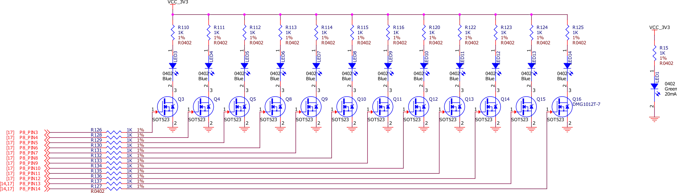
Fig. 326 User LEDs and power LED#
User and reset button#
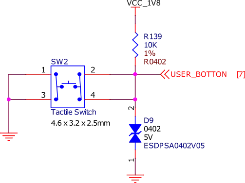
Fig. 327 User button#
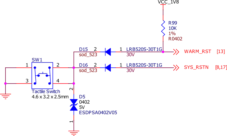
Fig. 328 Reset button#
Connectivity#
Ethernet#
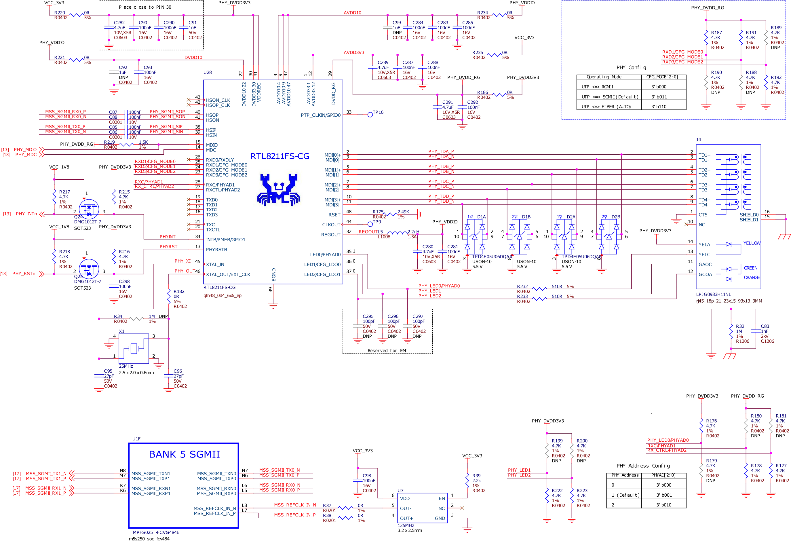
Fig. 329 Gigabit ethernet#
Memory, Media and Data storage#
DDR memory#
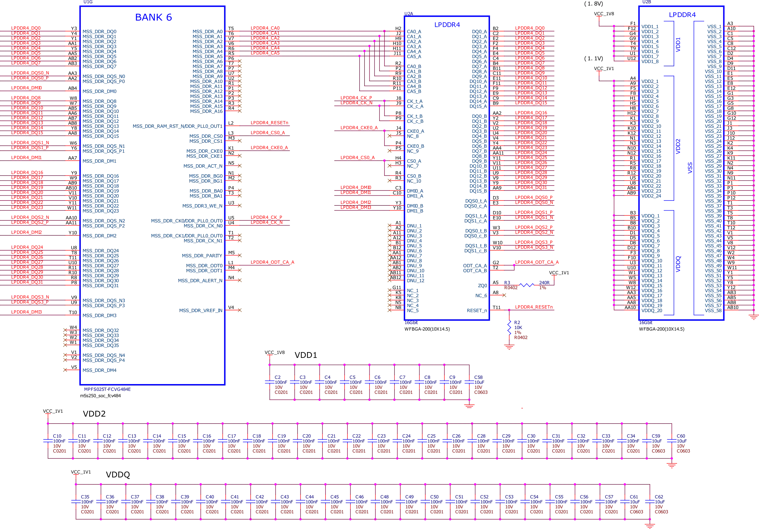
Fig. 330 LPDDR memory#
eMMC#
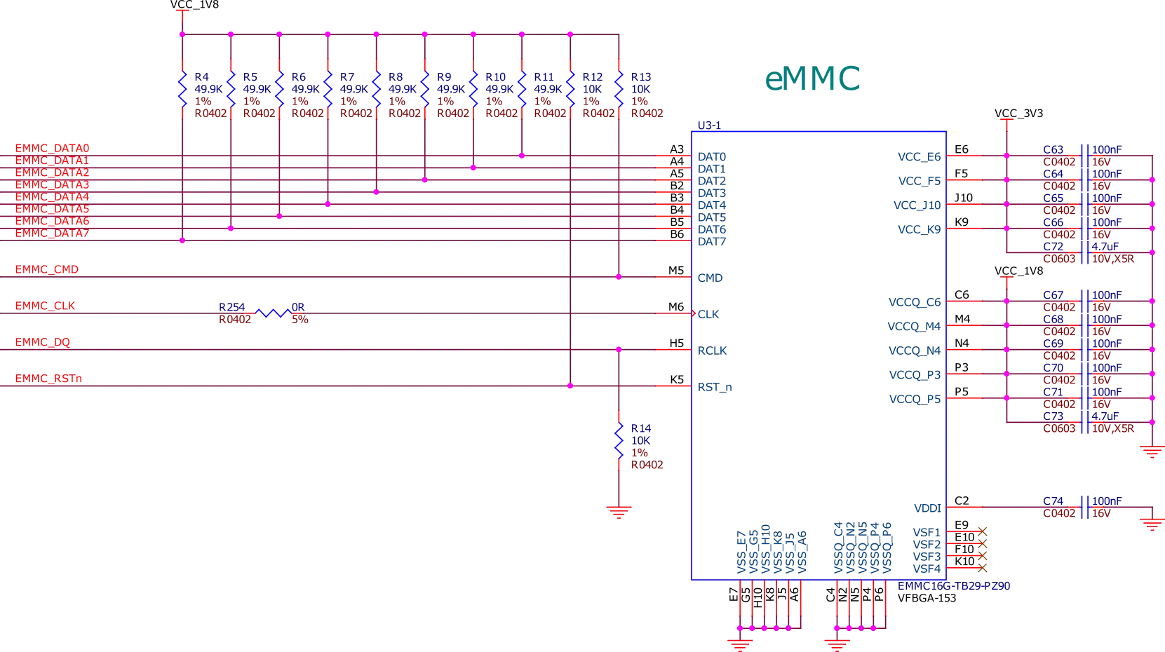
Fig. 331 EMMC flash storage#
microSD#
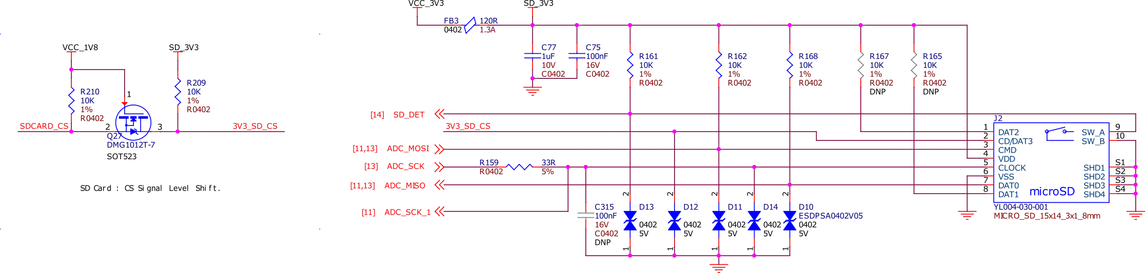
Fig. 332 SD Card socket#
EEPROM#
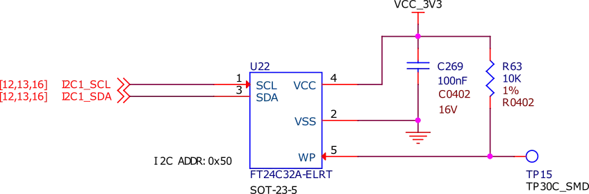
Fig. 333 EEPROM#
SPI flash#
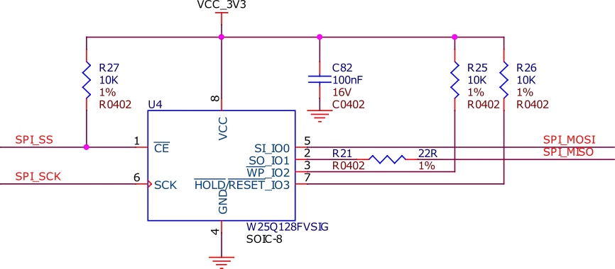
Fig. 334 SPI Flash#
Multimedia I/O#
CSI#
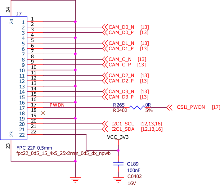
Fig. 335 CSI#
Debug#
UART debug port#
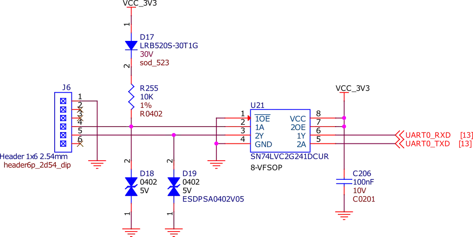
Fig. 336 UART debug header#
JTAG debug port#
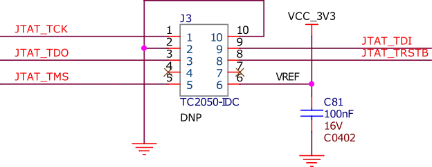
Fig. 337 JTAG debug header#
Mechanical Specifications#
Parameter |
Values |
|---|---|
Size |
86.38 * 54.61 * 18.8 mm |
Max heigh |
18.8 mm |
PCB Size |
86.38 * 54.6 mm |
PCB Layers |
12 Layers |
PCB Thickness |
1.6 mm |
RoHS compliant |
Yes |
Gross Weight |
106 g |
Net weight |
45.8 g |
